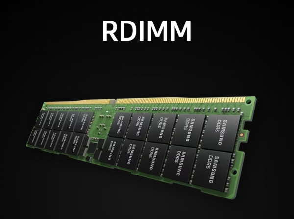
Samsung is considering incorporating molded-in-fill (MUF) technology in its upcoming generation of dynamic random-access memory (DRAM), as reported by TheElec. This move signifies Samsung’s exploration of innovative techniques to enhance the performance and efficiency of its memory solutions. MUF technology, previously utilized by SK Hynix in high-bandwidth memory (HBM) production, offers promising prospects for Samsung’s future DRAM endeavors.

Samsung’s tests on an MR MUF process have shown promising results
MUF technology involves injecting a material between semiconductors after drilling numerous tiny holes in the semiconductor layers. This process aims to securely connect multiple vertically stacked semiconductors. Samsung’s recent tests on an MR MUF process for 3D stacked memory have shown enhanced throughput compared to conventional methods like thermal pressed non-conductive film (TC NCF). However, there are considerations regarding its impact on physical characteristics.
While Samsung found MUF unsuitable for HBM technology due to specific requirements, it sees potential applications in 3DS registered dual in-line memory modules (RDIMMs), primarily used in server environments. The decision aligns with Samsung’s commitment to advancing server DRAM memory technologies to meet evolving industry demands.
MUF’s success in HBM production by SK Hynix has garnered attention in the semiconductor industry. This epoxy resin molding compound is believed to offer advantages such as preventing wafer warpage and enhancing overall performance. Samsung’s pursuit of developing its own MUF compound in collaboration with Samsung SDI indicates a strategic move to establish proprietary solutions tailored to its requirements.
The potential adoption of MUF technology by Samsung holds significance for the semiconductor market. As the world’s leading storage semiconductor company, Samsung’s endorsement of MUF could catalyze its widespread acceptance and adoption as a mainstream technology. This development has the potential to reshape the semiconductor material market landscape, driving significant transformations in the industry.
Related:
- Big Discount: AOOSTAR R1 N100 NAS Mini PC Only For $159
- Get latest Oneplus 12 Phone for $699 on Geekwills
- Get $100 Off on Vivo X100 Pro at Giztop
- Get the Realme GT5 Pro phone on Giztop for $599
- Xiaomi 13 Ultra Premium Camera Phone is now only $799
(Source)


Comments