
Add GIZMOCHINA as Preferred Source on Google
Huawei is proposing a new way to keep the semiconductor industry moving forward at a time when making smaller and smaller chips is becoming increasingly difficult.
At the International Circuit Systems Symposium (ISCAS) 2026 hosted by the Institute of Electrical and Electronics Engineers, Huawei executive He Tingbo introduced what the company calls the “Tau (τ) Law.” It’s a new principle that Huawei says could eventually help chips reach performance levels similar to future 1.4nm processors by 2031.

For decades, the chip industry has relied on Moore’s Law, which says more transistors can be packed into chips every few years by shrinking their size. This approach has helped smartphones, laptops, and AI systems become faster and more efficient over time.
However, the industry is now approaching physical and financial limits. Making chips smaller is becoming far more expensive, while performance gains are no longer arriving at the same pace as before.
What is Huawei’s Tau Law for semiconductors?
Huawei says its Tau Law could offer another path.
Instead of depending mainly on “geometric shrinkage,” or physically making transistors smaller, the company wants to focus on “time shrinkage.” In simple terms, Huawei is trying to reduce the amount of time signals need to travel inside a chip. The shorter the delay, the faster and more efficient the processor can become.
A major part of this strategy is something Huawei calls “logic folding.” You can compare this to folding a long road into multiple compact layers so cars can reach destinations faster without increasing travel distance. In semiconductors, folding chip logic could help reduce signal delay while also increasing transistor density.
Huawei says this system works across several layers at once, including devices, circuits, chips, and full computing systems. According to He Tingbo, President of Huawei Semiconductor Business, the company has already designed and mass-produced 381 chips over the past six years using ideas connected to this new approach.
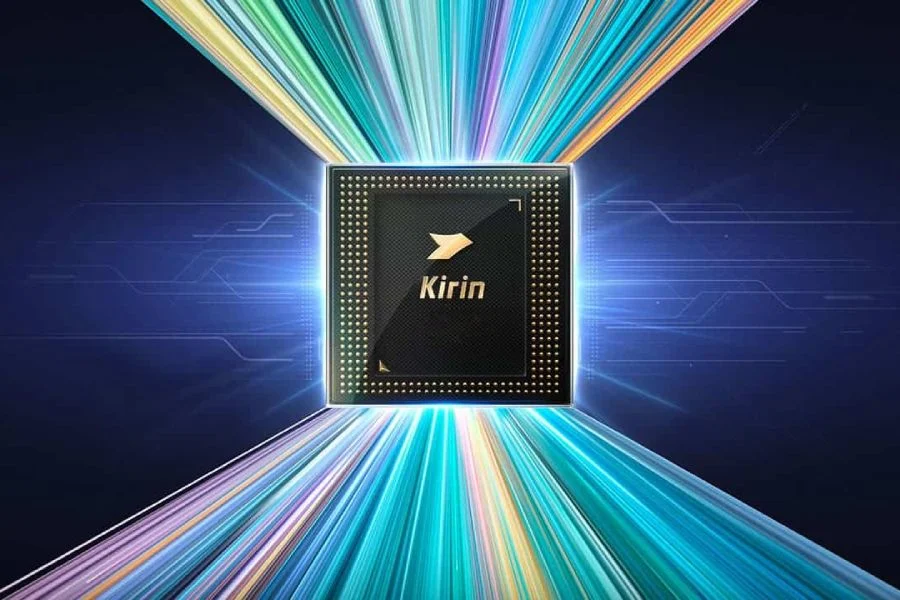
The first major commercial product using logic folding will reportedly be Huawei’s next Kirin 2026 mobile chip, expected to launch later this autumn. Huawei claims the technology will significantly improve performance and energy efficiency.
The company also believes that chips developed under Tau Law could eventually achieve a transistor density equivalent to advanced 1.4nm process technology within the next five years.
Mind you, this does not necessarily mean Huawei will physically manufacture a true 1.4nm chip using traditional methods. Instead, the company is arguing that smarter chip architecture and signal optimization could deliver similar levels of computing capability.
Huawei also used the event to emphasize cooperation, with He Tingbo saying that no single company can solve the semiconductor industry’s challenges alone.
For more daily updates, please visit our News Section.
Stay ahead in tech! Join our Telegram community and sign up for our daily newsletter of top stories.




Comments