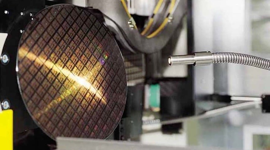
TSMC (Taiwan Semiconductor Manufacturing Company) is on track with its 3nm process technology. The company is on schedule with its development and plans on beginning the risk production phase within this year.
In a conference call earlier this week, the chipmaking giant’s CEO CC Wei stated that ” Our N3 technology development is on track with good progress. We are seeing a much higher level of customer engagement for both HPC and smartphone application at N3 as compared with N5 and N7 at a similar stage.” Furthermore, the company aims on starting mass production by the second half of 2022, with the risk production starting in the second half of this year.

According to a DigiTimes report, TSMC has also set its Capex target at 25 to 28 billion US Dollars, which is higher than the previously estimated 20 to 22 billion US Dollars. The reason for the hike is currently unknown as the company’s CEO refrained from commenting on specific orders and customers when asked about receiving outsourcing demand from Intel. However, Wei added that TSMC’s Capex intensity is high due to technical complexity.
Editor’s Pick: Apple App Store in China removed nearly 50,000 games in December 2020
As per the senior executive, the expenditure on EUV lithography and its technological advancements is a major reason for the higher Capex this year. Additionally, TSMC believes that a higher levels of expenditure on capacity will be helpful towards future growth as well. Similarly, the world’s largest contract chipmaker has also raised its CAGR target for revenue to 10 to 15 percent in US dollar term through 2025.

TSMC has also disclosed that it is working on its 3D SoIC (system on integrated chips) packaging technology, which will be ready for production in 2022. The company is expecting its revenue from backend services to grow as well within the next few years, especially with its 3DFabric family of technologies that it has been promoting. Wei further added that “We observe chiplets are becoming an industry trend. We are working with several customers on 3DFabric to enable chiplet architecture.”
UP NEXT: OPPO A93 5G with 90Hz display, Snapdragon 480, 48MP triple cameras launched in China


