Semi-conductor foundry, GlobalFoundries (GF) is one of the popular semi-conductor foundries alongside TSMC (Taiwan Semi-Conductor Manufacturing Company) and Samsung. They are Apple’s second source manufacturer and also known to build AMD’s 14nm Polaris GPU. The company has had it rough for a few years with respect to building its own processing technology but are planning to make a comeback with a new 7nm FinFET process.
The interesting thing about the new process technology is that GlobalFoundries will use a full node shrink instead of a hybrid node. If you do not know what the differences between both nodes are, I”ll attempt to break it down to the best of my knowledge in the next paragraph.

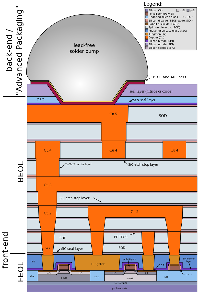
The process of semiconductor manufacturing can be split into three major steps:
- Front-End-of-Line (FEOL): this is the process of manufacturing transistors. It encompasses wafer production, lithography, and deposition
- Back-End-of-Line (BEOL): This is the process of connecting together the individual parts of a chips.
- Packaging
Samsung and TSMC are two semiconductor foundries that use hybrid nodes (14/16nm). What they do is combine a new transistor architecture (FEOL) with an already established set of design rules for how those transistors are connected together (BEOL). Shrinking or altering of FEOL and BEOL at the same time results in a full node.
READ MORE: Real Images of Samsung ”Veyron” SM-2017 Flip Phone
Intel is the only company that actually sticks to full-node shrinks when they introduce a new technology. GF wants to replicate this process for the 7nm node, jumping 10nm in doing so.
The reason for doing so is because the 10nm process is said to be a short-term node according to TSMC and based on a statement made by the CEO of GlobalFoundries, Sanjay Jha ”the industry is converging on a 7nm FinFET as the next long-lived chip.


